RP2040 as a 100MSPS Logic Analyzer via Programmable I/O State Machines
Examining how Raspberry Pi’s RP2040 dual-core microcontroller utilizes its PIO hardware state machines and DMA streaming to capture 100MSPS digital signals with PulseView & Sigrok integration.
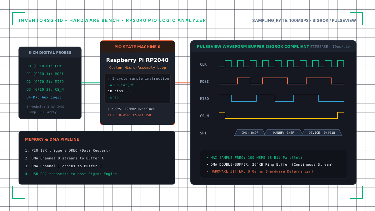
Digital Signal Capture at Silicon Cost
Dedicated multi-channel logic analyzers frequently represent an expensive investment for students and hardware developers. While USB-based FX2-style logic analyzers exist, their streaming capabilities are bottlenecked by high-speed USB 2.0 PHY constraints and fixed capture timing.
The Raspberry Pi RP2040 microcontroller presents a unique architectural advantage: Programmable I/O (PIO) blocks. By implementing dedicated state machines that bypass CPU execution entirely during acquisition, the RP2040 can operate as a continuous 8-channel or 16-channel digital capture instrument operating at up to 100 Megasamples per second (MSPS).
How RP2040 PIO Bypasses Core Execution Bottlenecks
Traditional microcontroller logic analyzers sample GPIO pins in a tight loop:
// Traditional CPU polling loop (Jitter prone & frequency limited)
while (capturing) {
    *buffer++ = sio_hw->gpio_in;
}
In contrast, the RP2040 includes two PIO blocks, each with four independent 32-bit state machines capable of executing 1 instruction per system clock cycle.
[ GPIO Input Pins (D0 - D7) ]
             │
             ▼
┌──────────────────────────────┐
│  PIO0 State Machine 0        │
│  - IN PINS, 8                │ ──▶ Samples every 1 clock cycle (10ns at 100MHz)
│  - PUSH (Auto-push at 32b)   │
└──────────────┬───────────────┘
               │ (32-bit Words via FIFO)
               ▼
┌──────────────────────────────┐
│  Direct Memory Access (DMA)  │
│  - Dual Ring Buffer Channels │ ──▶ Zero CPU intervention
│  - Writes to 264KB SRAM      │
└──────────────┬───────────────┘
               │
               ▼
┌──────────────────────────────┐
│  Core 1 USB Streaming        │ ──▶ USB Bulk Endpoints to Sigrok / PulseView
└──────────────────────────────┘
The state machine assembly code required for deterministic 8-bit capture is just a single instruction:
.program logic_capture
.wrap_target
    in pins, 8
.wrap
With PIO autopush enabled at a threshold of 32 bits, the state machine packs four 8-bit samples into a single 32-bit word and transfers it directly into the RX FIFO without a single CPU cycle.
Memory Allocation & DMA Ping-Pong Streaming
The RP2040 features 264 KB of on-chip SRAM split across multiple striped banks. To sustain continuous high-speed captures without dropouts:
At 100 MSPS with 8 channels (1 byte per sample), the raw data throughput is 100 MB/s. Because full-speed USB 1.1 on the RP2040 is capped at 12 Mbps, ultra-high-speed captures (50MSPS–100MSPS) utilize the internal SRAM as a circular sample buffer, while continuous live streaming is supported up to 2MSPS.
Protocol Decoding with Sigrok & PulseView
The firmware implements the standard Sump / Openbench Logic Sniffer (OLS) protocol over USB CDC. When connected to a computer running Sigrok or PulseView, the device is instantly recognized as an 8/16-channel analyzer with native protocol decoders for:
- I2C, SPI, and UART
- CAN Bus and LIN
- SWD / JTAG debug streams
- WS2812B / Neopixel timing verification
Critical Engineering Trade-offs & Practical Notes
Source Documentation & Integrity Notice
InventorsGrid adheres to strict hardware journalism standards. This analysis was conducted by dissecting official schematics, firmware repositories, component datasheets, and primary documentation. We do not claim to have physically benchmarked or fabricated this hardware unless lab measurements are explicitly stated.